

Focusing on FPGA image solution customization

FPGA simulated MIPI camera, successfully connectedNVIDIAAGX Developer
Visual cameras are key to machine intelligence/automation, and NVIDIA Jetson supports cameras from multiple partners, including cameras with USB, Ethernet, MIPI, and other interfaces. Jetson provides a complete Jetpack SDK for these cameras, enabling users to quickly connect to these cameras and implement corresponding designs.
The list of cameras supported by Jetson can be found on the official website as follows:
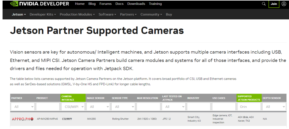
Select the CSI/MIPI interface and Orin suite, and the webpage will display a list of Jetson Partner supported cameras, mainly Sony's IMX290 IMX334、IMX179、IMX335、IMX415 , And Aptina's AR0234, AR0144, AR0822, etc. Therefore, for example, if users use NVIDIA's Jetson AGX Orin developer suite, the SDK of the suite natively supports CSI access to the sensors listed above, allowing users to quickly develop their own solutions.
![]()
If you choose the camera from the above list and use it with the accompanying CSI adapter board, as the Camera Partner has already pre docked with various models of NVIDIA Jetson, the driver in the original factory image is already supported by default, and can be plug and play.
howeverIf we choose a sensor model outside the list, which is not a Camera Partner product, we cannot directly use it,For example, if I want to use Sony's IMX472, IMX252, Sitewe's SC2210, SC235HGS, etc., thenIt is necessary to upgrade the supporting hardware and driver software.For this, Aoweisi provides you with a complete solution, which can be equipped with any camera or choose FPGA integrated ISP.
As shown in the following figure: The scheme adopts Yilingsi Titanium 16nm FPGA Ti60F225, collects image sensor data through MIPI CSI RX, undergoes a series of complex ISP operations inside the FPGA, and then sends the image data to the backend through MIPI CSI TX.

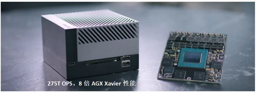
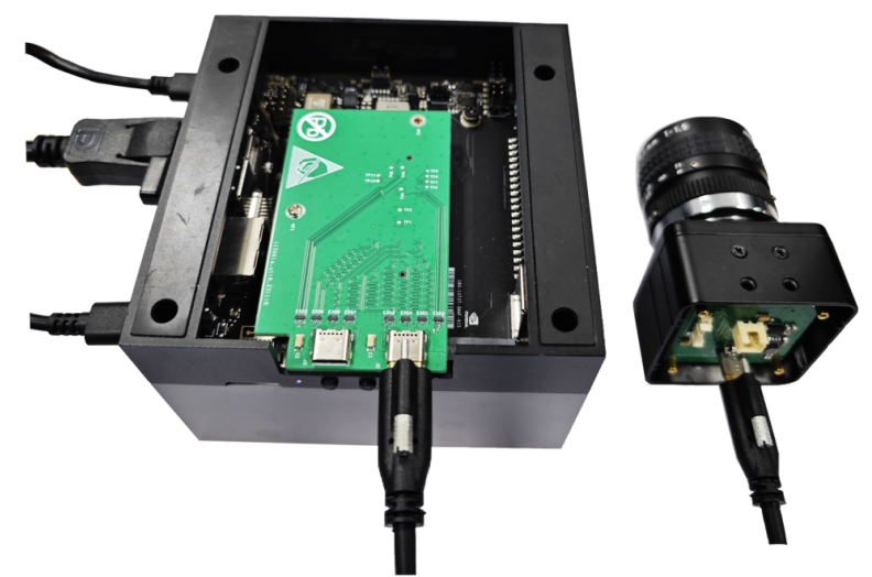
Among them, VC-MIPI-AGX is the MIPI access sub card of the NVIDIA Jetson AGX Orin developer kit developed by Aoweisi. As shown in the figure below, it is the MIPI card slot of AGX and the access sub card we designed. We use a high-speed and stable TypeC 3.0 data cable to transmit MIPI signals. The current solution can support 2 MIPI CSI channels, with a maximum bandwidth of 6Gbps per channel. At present, the solution has been successfully integrated into AGX, stable and reliable, and the baking machine has passed the test.

The low power consumption, high bandwidth, and small size characteristics of the Yilingsi 16nm titanium series FPGA fully empower terminal products to make them innovative and competitive. The titanium series Ti60 can support multi camera input, multi type screen driver, high-performance RISC-V soft core and other functions with MIPI/LVDS interfaces, suitable for various camera and sensor systems and other scene applications.

Therefore, we chose Yilingsi's FPGA as the main controller, fully utilizing its high-speed and low-power characteristics to complete the collection of MIPI CSI, ISP image processing, and transmission of MIPI CSI. The MIPI PHY of Yilingsi Ti60 FPGA is 1.5Gbps single channel, and 4 lanes support 6Gbps. At 85% effective bandwidth, the effective transmission resolution/frame rate is evaluated as follows:
|
RGB888 transmission |
Effective bandwidth |
Actual bandwidth (85%) |
result |
|
RGB888 24bit transmission |
|||
|
1920* 1080@60 |
Effective bandwidth=1920 * 1080 * 8bit * 60 * 3=2.986Gbps |
3.513Gbps |
√ |
|
1920* 1080@100 |
Effective bandwidth=1920 * 1080 * 8bit * 100 * 3=5.286Gbps |
6.219Gbps |
X |
|
1920* 1080@120 |
Effective bandwidth=1920 * 1080 * 8bit * 120 * 3=5.972Gbps |
7.026Gbps |
X |
|
Bayer 8-bit transmission |
|||
|
1920* 1080@60 |
Effective bandwidth=1920 * 1080 * 8bit * 60=0.9953Gbps |
1.171Gbps |
√ |
|
1920* 1080@100 |
Effective bandwidth=1920 * 1080 * 8bit * 100=1.659Gbps |
1.952Gbps |
√ |
|
1920* 1080@120 |
Effective bandwidth=1920 * 1080 * 8bit * 120=1.991Gbps |
2.342Gbps |
√ |
|
4096* 2304@60 |
Effective bandwidth=1920 * 1080 * 8bit * 60=4.530Gbps |
5.330Gbps |
√ |
Adopting RGB888 or Bayer 8-bit transmission has its advantages and disadvantages:
1) RGB888 8-bit transmission, AGX can directly obtain image data, with the advantage of no additional source data processing overhead; The downside is that due to Bayer's 3x bandwidth, the current FPGA scheme can only support up to 1080P60 scheme.
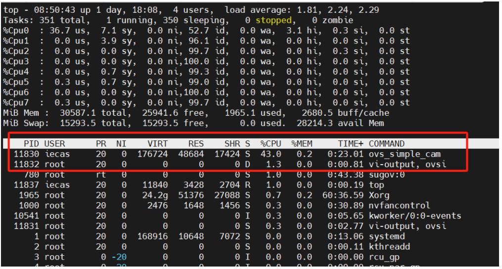
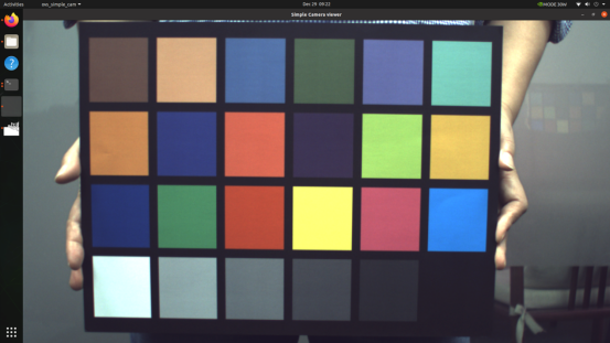
2) Bayer 8-bit transmission, with a bandwidth of 1/3 of RGB888, can support higher resolutions (4K60), and at the same resolution, can support longer transmission distances than RGB888; The shortcoming is that AGX's CPU (Neon) is needed to process the Bayer2RGB algorithm. Currently, testing 1080P120 consumes 43% of the resources of one CPU (a total of 12 CPUs, with single core resource consumption as shown in the following figure).
Based on comprehensive evaluation, due to the current use of only one AGX CPU and the user's algorithm mainly running CUDA on the GPU, the advantage of using Bayer transmission is more obvious.
NVIDIA can also perform complete ISP image processing, and even the ISP function and performance implemented by ASIC are more powerful than FPGA. However, in this solution, we have to use FPGA for complete ISP processing, mainly for the following reasons:
1) NVIDIA still requires a lot of tuning work for the selected sensors;
2) NVIDIA's ISP does not support 8-bit RAW input mode;
3) Some application engineers are not familiar with the ISP field;
4) Some ISP algorithms are not included in NVIDIA;
5) The demand for low latency requires a pipeline to complete ISP.
In view of this, we have completed a complete ISP processing process using FPGA. MIPI CSI directly outputs the data after FPGA image processing. After NVIDIA AGX receives the RGB data, users can directly carry out subsequent application algorithms. The ISP image processing pipeline based on Yilingsi FPGA is as follows:
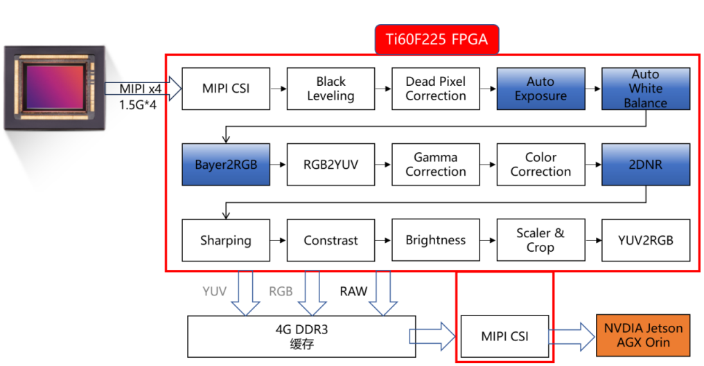
The self-developed assembly line ISP by Aoweisi and its related features are shown in the table below:
|
parameter |
describe |
Parameter switch |
|
Black Leveling |
Black level correction |
|
|
Dead Pixel Correction |
Bad Point Correction Module (DPC) |
|
|
Auto Exposure |
Automatic exposure algorithm module |
U adjustable switch U AE brightness target value U AE sensitivity |
|
Auto White Balance |
Automatic white balance algorithm module |
|
|
Bayer2RGB |
Bayer to RGB domain |
|
|
RGB2YUV |
RGB to YUV domain |
|
|
Gamma Correction |
YUV domain Gamma correction |
U adjustable parameters |
|
Color Correction |
RGB color correction |
|
|
2DNR |
2D noise reduction algorithm module |
U adjustable switch U adjustable strength |
|
Sharping |
Edge sharpening module |
U adjustable switch U adjustable strength |
|
Saturation |
Saturation adjustment |
U adjustable strength |
|
Contrast |
Contrast enhancement module |
U adjustable strength |
|
Brightness |
Brightness adjustment module |
U adjustable strength |
|
Scaler&Crop |
Zoom/Screenshot Module |
U adjustable parameters |
|
YUV2RGB |
YUV to RGB module |
In terms of hardware, the VC-MIPI-AGX sub card designed by Ovis is used to achieve user MIPICSI to AGX Samtec input. In terms of software, it is necessary to develop specific Sensor driver adaptations based on hardware board and module design. If there are special customized control requirements, such as ISP parameter control, it is necessary to modify the Camera framework for deep customization development.
For the protection of system security, Jetson's kernel compilation was turned on when it left the factoryDriver Signature OptionsIf the newly developed driver signature certificate does not match, the driver ko file cannot be loaded. However, most users are unable to obtain the signature certificate from NVIDIA when compiling factory images, which cannot solve the ko signature problem. If you need to use a new sensor module, you will need toRecompile the kernel, generate a full system image, and burnsystemThe workload is quite enormous.
Aoweisi solves the above-mentioned software and hardware problems for customers and creatively uses typeC 3.0 cables as data transmission media, with reliable connections and stable communication. Based on the NVIDIA Jetson AGX Orin developer platform, the self-developed FPGA MIPI ISP camera connection environment is connected as follows:
Function
Programme
SZOVS,Born for FPGA images…
Buy NowDetailed introduction
基于易灵思国产FPGA,实现六目同步1080P实时采集+成像系统

简而言之,基于FPGA实现单目的采集,并没有什么难的。
但基于FPGA,实现多目的同步采集→存储→显示,就不是那么好做了。具体分析,有难点如下:
实现6目同步采集需要一定经验
实现6路ISP图像处理资源消耗很大
实现6路同时缩放再拼接到1080P麻烦
实现触发拍照存储SD卡难度大
如何保证系统稳定可靠更难
综上一切,系统实现并不是那么容易的。
但当FPGA来临,再多的困难,也充满了机遇。

于是乎,我们基于国产易灵思FPGA(钛金Ti60F225),实现了6目1080P同时采集→存储→显示的系统,如下所示:
.png")
如图所示,是奥唯思设计的,基于GW5AT-LV60 FPGA的图像开发板。开发板采用核心板与底板的分离设计,方便客户扩展及未来底版升级设计。
系统采用如下主要元件:

最终,我们在3.1W的功耗下,实现了同步并行采集存储+显示的系统。
同样的功能,在Xilinx ZYNQ7020上,需要将近5.2W的功耗,足以见得,16nm易灵思钛金FPGA在功耗上的显著优势。
此外,采用FPGA实现6目采集+存储+显示,最大的价值在于:
流水线计算,几乎没有延时
完全的同步,相机间没有时差
自定义ISP,非常的灵活
随时可加后处理算法,想象空间大
总结一句话,FPGA的价值所在,就是to be the one,即实现ARM做不到的性能,成为那个不可替代的角!
.png")
探索未知,永无止境;
掌握了FPGA,真的可以掌握整个世界:
试想,6目同步ISP相机,可以以什么样的姿态,翱翔天空呢?
HDMI 1080P60可用于无线图传
触发/同步保存原图可用于拍摄存图
不同的的镜头可用于监测不同的视场/波段
不同的角度安装更可以实现720°同步采集
.png")
奥唯思,专注FPGA图像开发。
作为易灵思的独家第三方合作伙伴,奥唯思在易灵思FPGA的视觉方案实现,以及技术推广上,做出了有目共睹的贡献。
如下是本系统采用的,基于易灵思钛金Ti60F225的FPGA开发平台,入手国产FPGA视频图像,易灵思以其独特的架构,以及16nm的工艺优势,在MIPI以及低功耗应用有着先天的优势。

淘宝采购链接:ttps://item.taobao.com/item.htm?ft=t&id=677237740535

2024,奥唯思推出了钛金Ti60F100拇指板,以及白菜价的20K Trion FPGA学习板,出席+演讲了易灵思+思特威视觉大会,并独家支持了国产FPGA大赛(易灵思赛道)。

2025,奥唯思将会更多的投入,主要包括如下几个方面:
出版《深入浅出玩转易灵思FPGA》一书
推广基于易灵思FPGA的RISC-V开发案例
独家研发TJ135 FPGA视频图像设计平台

 302, Building 17, Nanshan Ruiyuan, Xili Longzhu 3rd Road, Nanshan District, Shenzhen City, Guangdong Province
 19926595670
 cb@szovs.com
 WeChat
 Skype
Skype
 Official WeChat
website

FPGA website
Official account
Official WeChat public account
Official account
Official account
Skype
Skype
Mailbox
cb@szovs.com
Comeback